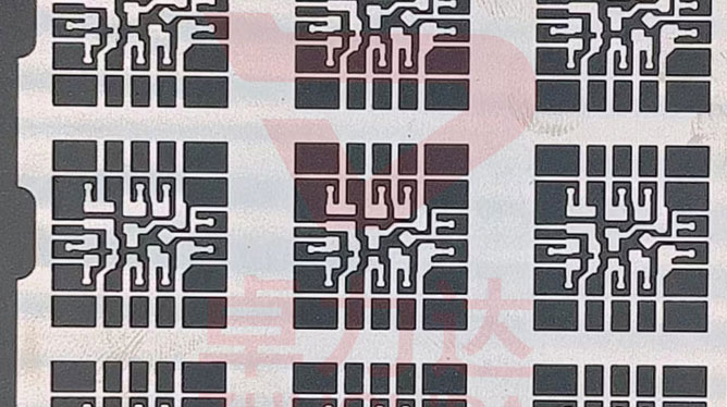
Semiconductor lead frame etching process is a complex and delicate process, the general steps are as follows:
1. Material Preparation: First of all, you need to prepare the appropriate amount of semiconductor lead frame needs to be etched material, usually metal or alloy, such as 4J42, 4J29 and so on. At the same time, in order to ensure the precision and effectiveness of the semiconductor lead frame etching process, you need to clean the surface to be etched to remove surface stains and oxides.
2. Coating resist: before the lead frame etching process, the lead frame surface needs to be coated with a layer of resist to protect the parts that do not need to be etched. Resist selection should be based on specific materials and etching requirements.
3. Graphics transfer: the semiconductor lead frame etching of the graphics need to be transferred to the metal lead frame material through photolithography. This step requires the use of photoresist and other materials, the use of exposure machines and exposure processing under specific lighting conditions.
4. Etching process: After transferring the graphics to the lead frame, the etching process can begin. According to different process requirements, you can choose dry etching or wet etching. Dry etching mainly using plasma etching, with high precision, high speed characteristics; wet etching is the use of chemical solutions for etching, with low cost, simple operation advantages.
5. Degumming: in the semiconductor lead frame etching is completed, the need to remove the surface of the residual photoresist and resist. This step is usually dissolved using a specific solvent to remove.
6. Post-processing: After the debinding process is completed, some subsequent processing, such as cleaning, drying, etc., in order to restore the original state of the lead frame.
On the semiconductor lead frame etching process accuracy, its accuracy is mainly affected by the following factors:
1. Equipment accuracy: the accuracy of the etching equipment has a crucial impact on the processing accuracy. Equipment mechanical errors, positioning errors and control system errors may affect the final etching accuracy.
2. Material properties: the physical and chemical properties of the lead frame material will also have an impact on the etching accuracy. For example, the hardness and toughness of the material, as well as the selection of resist, etc. may affect the effect and accuracy of etching.
3. Process parameters: the choice of etching process parameters have a great impact on processing accuracy. For example, etching time, gas flow, solution concentration and other parameters will affect the depth of etching and contour.
4. Environmental factors: environmental temperature, humidity and cleanliness will also have an impact on the accuracy of the semiconductor lead frame etching process. Therefore, the need for etching processing in a stable process environment.
In order to improve the accuracy of the etching process, the following measures can be taken:
1. Select high-precision etching equipment, and conduct regular equipment maintenance and calibration to ensure the stability and accuracy of the equipment.
2. Select the appropriate resist and process parameters according to the specific material and process requirements, and carry out strict process control.
3. Before the etching process, the surface to be processed is strictly cleaned to reduce the impact of pollution and impurities on the etching.
4. Maintain a stable process environment, such as temperature, humidity and cleanliness, in order to reduce the impact of environmental factors on the etching process.
5. Regular quality inspection and control, timely detection and treatment of problems to ensure that the quality and accuracy of the final product meets the requirements.
In summary, semiconductor lead frame etching processing is a complex and delicate process that requires multiple steps and links. In order to improve the processing accuracy, it needs to be controlled and managed from multiple aspects such as equipment, materials, process parameters and environment. At the same time, strict quality inspection and control is also an important means to ensure the quality of the final product.
Contact: andy_Lai
Phone: 18938693450
E-mail: yw9@zldsmt.com
Add: Building A3, Huafa Industrial Park, Fuyong Town, Fuyuan Road, Fuyong Town, Baoan District, Shenzhen,China