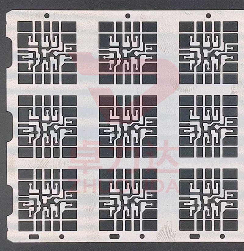
Do you know about leadframe etching processing? This high-precision processing technology is not a general cow! Let us unveil its mysterious veil today.
Lead frame etching is a widely used in the field of microelectronics processing technology, the principle is that the film through the mask, exposure, development and other multi-channel process,
so that the conductive layer on the formation of a certain shape and size of the wire structure. This processing technology is widely used in integrated circuits, MEMS and other fields, and its processing
accuracy reaches the sub-micron level, becoming an indispensable part of today's microelectronics manufacturing.
In leadframe etching processing, the most critical link is the mask technology. The quality of the mask directly determines the precision and reliability of the lead structure. In order to ensure the quality of the mask,
scientists have developed a variety of mask materials and preparation processes. Among them, photolithography is currently the most widely used mask technology, its resolution can reach the sub-micron level, known
as the microelectronics manufacturing "soul".
Leadframe etching processing, this technology has an important position in the field of microelectronics. Its high processing precision, low manufacturing cost, by a wide range of applications and concerns.
Have you guys heard of this technology? Come to leave a comment and share your thoughts with us!
Contact: andy_Lai
Phone: 18938693450
E-mail: yw9@zldsmt.com
Add: Building A3, Huafa Industrial Park, Fuyong Town, Fuyuan Road, Fuyong Town, Baoan District, Shenzhen,China